CATEGORIES
Alumina thin films: Structure and Common USES
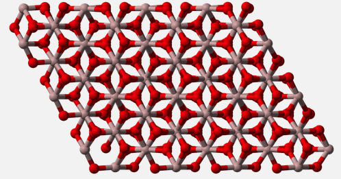
The most common structure of alumina (Al2O3) is known as corundum, which is its thermodynamic stable form. It is a hexagonal close-packed structure.
Alumina thin film coatings often have a polymorph structure consisting of clusters of tiny crystals of different sizes. There is knowledge about the various crystalline structures in which alumina can grow. But they are very difficult to characterize in a thin film.
Alumina thin films have multiple uses. A more porous structure is preferred for the manufacturing of catalysts. In the world of microelectronics, Al2O3 thin films are often used for tunnel barriers or dielectric optical coatings.

The hexagonal close-packed structure of alumina in a ball and stick scheme in which the oxygen atoms are red and the aluminum atoms are pale pink.
Tunnel Barriers
Since alumina has a high electrical insulation paired with relatively high thermal conductivity it is a natural choice for tunnel barriers. The challenge for this type of films, that are preferably as thin as possible, is to avoid the creation of pinholes that allow leakage currents. In some processes, the aluminum is coated in a DC sputtering system, while the Al2O3 is created by oxidizing the aluminum layer after the coating (for instance by placing the wafer in a water steam environment). A thin layer of few nanometers of Al2O3 on any Al surface is common unless protected, but the hot water steam is used to increase the depth of the oxidization. Although this system has its advantages, reactively sputtered Al2O3 thin films with an ECR plasma sputtering coating system can show up to 100 times lower leakage current density.

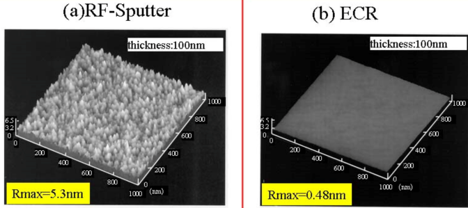
In this comparison of the thin film roughness (film thickness just 100nm) by a RF sputter with and without ECR plasma coating tool clearly depicts the advantages of an additional non-mechanical energy input into the growing film. The rough film on the left is likely to develop pin holes and have poor leakage current properties as compared to the smooth and dense film on the right with ECR plasma.
Thin Film Alumina in optical applications
For optical applications, Al2O3 is one of the most common coatings due to its transparency on a broad wavelength range and the refraction index of 1.7nm. It is a typical component of dielectric mirrors with a combination of two dielectric thin films with alternating refractive indexes. By combination of thickness and refractive indexes at certain ratios, highly efficient mirrors can be created for instance for laser diodes.
When the thin film is formed by coating in a vacuum chamber, the very first stage of thin film growth is a nucleation phase in which the incoming species of AlxOy at the substrate adjust to the substrate lattice pattern. The actual separation distances in the Al2O3 hexagonal close packed structure, or the lattice shape that the Al2O3 would form by itself in an ideal world and the substrate lattice distance are different.
Depending on the mobility that the AlxOy species have once they attach to the substrate, a polymorphic structure with smaller or larger clusters of corundum or other known alumina structures will form with larger or smaller interstitial volumes. In coatings with relatively low impact energies and low thin film energy, a columnar like structure with empty spaces that propagate even up to 100nm will render an Al2O3 coating with rough surface and low refraction index. The interstitial spaces could eventually become homes for air humidity, rendering the optical properties of the film environment dependent.

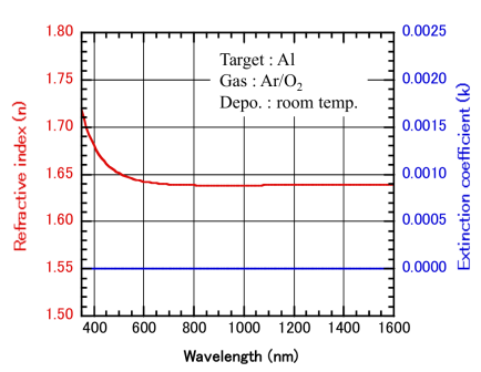
Alumina thin film characterization (100nm thickness) deposited in an ECR plasma sputter coating tool. The refractive index at 550nm is around 1.64 and the extinction coefficient (absorbpion) is below k=10-4 close to the theoretical value for bulk alumina.
Coating Systems for Alumina thin films
Some coating systems for thin film alumina coating provide high energetic particles targeted towards the substrate. This can be the AlxOy species themselves or an additional plasma consisting of Ar projectiles. Either way, the function of these projectiles is always that the film is compacted, the crystalline components of the polymorphic film are made smaller and the refraction index of the thin film raises to near bulk parameters. A post-coating annealing step at high temperatures additionally helps the deposited film to further transform into the desired corundum structure.
In the ECR plasma sputtering coating system, the projectiles of AlxOy reaching the substrate have enough energy to compact the growing film. Yet, the additional energy provided by the large amount of energetic electrons from the ECR plasma helps with the adatom mobility of the AlxOy species on the substrate. The result is a very smooth film and virtually no damage to the underlying substrate at ambient temperatures.
An additional positive feature is the strong suppression of selective sputtering of the AlxOy film by the incoming species. This would preferentially sputter the oxygen away, making the film deviate from its stoichiometric balance and slightly increasing the thin film optical absorption. The result is a full stoichiometric film with absorption index below k=10-4 and refraction index of n=1,67 even below 100nm thickness.

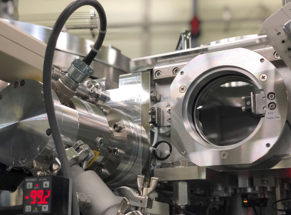
The ECR plasma sputtering coating system by Mitsui Knwoledge Industry provides the growing alumina film with the needed energy without damaging the substrate on which it is growing.
Do you like what you see?
We value your feedback, so let us know what you think!
Let us also know which topics you would like to see expanded.
Just give us a call, send us an e-mail or use the form to contact us.
